Solid-state
devices rely on the control of the flow of electrons and holes at the interface
(“heterojunction”)
formed between different semiconductors. Silicon is the workhorse of the
semiconductor industry. However, until now, creating a heterojunction
between Si and other materials with a larger energy gap has been an intractable
problem for the most part, because of the lack of a lattice match between Si
and crystalline wide-gap materials. In this seed, Sturm, Kahn, Schwartz and Loo report two materials that do
the job with complementary functionality, using polymers and inorganic amorphous materials to overcome
the lattice-match constraint. The organic semiconductor P3HT has a bandgap much
wider than that of Si. Due to the appropriate alignment of the band edges, PCCM
researchers show [1] that P3HT is an electron blocker, but transmits holes
efficiently (Fig. 1A). Conversely, amorphous TiO2 acts
as a hole blocker while efficiently transmitting electrons (Fig. 1B) [2]. Both
functionalities, crucial in photovoltaic devices, show the direction towards
high-efficiency low-cost cells based on silicon.
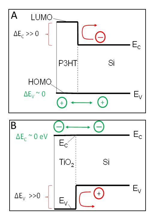
Fig. 1A The energy band edges Ec
and Ev
in P3HT/Si heterojunction.
When the highest occupied band (HOMO) of P3HT is aligned with Ev
in Si, electron flow is blocked, but holes are transmitted. Panel 1B shows hole
blocking in the complementary TiO2/Si
heterojunction.