We investigated the electronic properties of interfaces between two laminated polymer films. The top polymer film (Fig. (a)) is transferred to a soft PDMS stamp, and laminated against the bottom film, previously spin-coated on a substrate. Using electron spectroscopy and Kelvin micro-probe techniques, we demonstrated that the process does not introduce any molecular shift due to interface dipole or surface states. We also showed that the interface is transparent to charge carrier transport, as shown in Fig. (b). The current injected from top or bottom electrode is the same for the single 70 nm film (black) and for the laminated 2x35 nm film (red) [1].
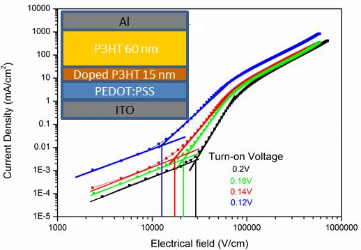
Extending this work, we investigated the lamination of two polymer films, one of which is as thin as 15 nm and is chemically doped to increase its conductivity and, in the case of p-doping, its work function (Fig. (c)). We demonstrated significant enhancement of charge injection in the undoped polymer, thus providing a very powerful and practical way to create ultra-thin doped interface areas at polymer/electrode interfaces.
(a)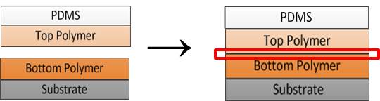
(b)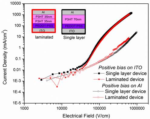
(c)