Graphene, a single atom-thin sheet of carbon, can be used to make ultra-fast electronics. Researchers at the University of Maryland Materials Research Science and Engineering Center (MRSEC) are collaborating with the U.S. Naval Research Laboratory (NRL) to understand how graphene forms on the surface of silicon carbide. Growing graphene on silicon carbide could provide a platform to manufacture high speed graphene transistors which could find uses in applications ranging from advanced radar to miniaturized cellphones.

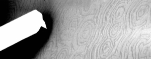
A scanning electron microscope image shows the atomic force microscope (AFM) tip (white) approaching the graphene surface. The wood-grain appearance of the surface is caused by the different graphene layer thicknesses – the AFM maps these differences in detail shown below.
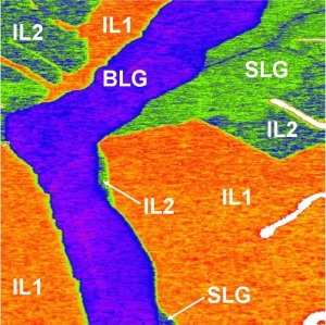
 A microscope technique called “Kelvin probe microscopy” (KPM) is used to map the differences in the electrical potential on the surface of graphene on silicon carbide, shown here as different colors. KPM identifies single layer graphene (SLG), bilayer graphene (BLG), and two types of interfacial layer (IL1 and IL2).