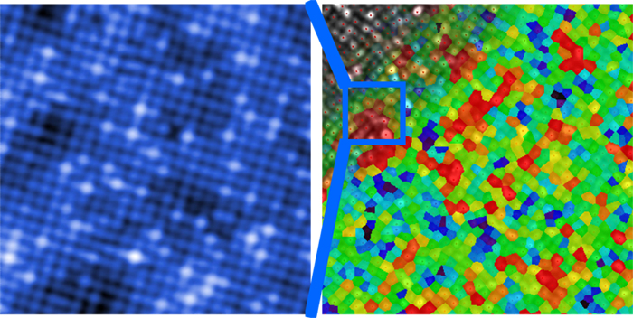
Professor Eric Hudson of the MIT MRSEC, along with members of his research group, and collaborators at Brookhaven National Laboratory and at Nagoya University in Japan, has developed a new method for probing electronic properties at the atomic scale. The scanning tunneling microscope, or STM, has been used for over two decades to image atoms in a variety of materials. Hudson's group has taken the technique one step further to measure with atomic precision electronic properties generally thought of as "bulk" (uniform throughout the sample), such as the "Fermi surface" - related to electron density. They found, surprisingly, that these properties actually vary from one atom to the next. Although still in the early stages of development, this work points towards a new understanding of a large class of novel materials, correlated electron systems, and of their many technologically relevant capabilities.
Image: The relative regularity of the atoms making up the high temperature superconductor Bi2Sr2CuO6+x, imaged (left) by scanning tunneling microscopy, hides tremendous nanoscale inhomogeneity of electronic properties, in particular electron density (determined and indicated in the colored map at right by the varying size of "electron waves" in the material).