Many of today’s electronic devices, including solar cells and transistors, are based on heterojunctions — precisely sculpted, atomic-scale interfaces between different materials. To reach the ultimate limit in miniaturization, scientists must learn to make these near-perfect unions in materials that are only a single atom in thickness.
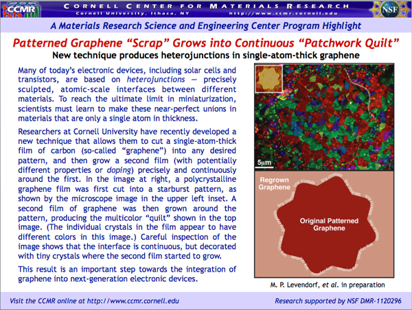
Researchers at Cornell University have recently developed a new technique that allows them to cut a single-atom-thick film of carbon (so-called “graphene”) into any desired pattern, and then grow a second film (with potentially different properties or doping) precisely and continuously around the first. In the image at right, a polycrystalline graphene film was first cut into a starburst pattern, as shown by the microscope image in the upper left inset. A second film of graphene was then grown around the pattern, producing the multicolor “quilt” shown in the top image. (The individual crystals in the film appear to have different colors in this image.) Careful inspection of the image shows that the interface is continuous, but decorated with tiny crystals where the second film started to grow.
This result is an important step towards the integration of graphene into next-generation electronic devices.