Field-effect transistors made of single organic crystals are ideal for studying the charge transport characteristics of organic semiconductor materials. Their outstanding device performance, relative to that of transistors made of organic thin films, makes them also attractive candidates for electronic applications such as active matrix displays and sensor arrays. The only approach currently available for creating single crystal devices is manual selection and placing of individual crystals—a process prohibitive for producing devices at high density and with reasonable throughput. We developed a method for effectively fabricating large arrays of single crystals of a wide range of organic semiconductor materials directly onto transistor source-drain electrodes. We fabricated large arrays of high-performance organic single-crystal field effect transistors with mobilities as high as 2.4 cm2/Vs and on/off ratios greater than 107, and devices on flexible substrates that retain their performance after significant bending. These results suggest that our fabrication approach constitutes a promising step that might ultimately allow us to utilize high-performance organic single crystal field-effect transistors for large-area electronics applications.
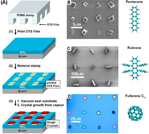
a, Schematic outline of the procedure: print with PDMS stamps with relief features that are inked with a thick OTS film and then press onto the substrates, place patterned substrate in vacuum-sealed tube in a temperature gradient furnace tube with the organic source material for growth of patterned single crystals. b, Patterned single crystal arrays of Pentacene c, Rubrene d, C60