 Researchers at OSU's Center for Emergent Materials have established a novel route for growing precise layers of optoelectronic 2D materials directly onto wafers commonly used by the semiconductor industry. This route combines the epitaxial growth of a crystalling precursor lattice (CaGe2) with its conversion into a layered 2D material (GeH) phase. This route is a powerful, controllable, and scalable strategy than can integrate precise thicknesses of 2D materials, with high material quality, directly into semiconductor processing technology.
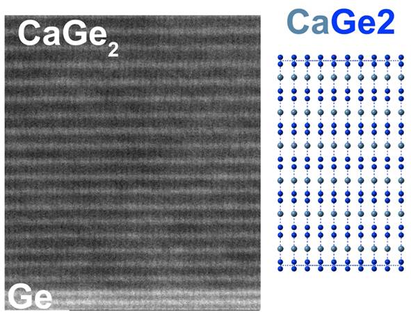
Two-dimensional crystals are an important class of materials for novel physics, chemistry, and engineering. Germanane (GeH), the germanium-based analogue of graphane (CH), is of particular interest due to its direct band gap and spin–orbit coupling. CEM researchers have established the successful co-deposition growth of CaGe2 films on Ge(111) substrates by molecular beam epitaxy and their subsequent conversion to germanane by immersion in hydrochloric acid. They utilized cross-sectional transmission electron microscopy (TEM), reflection high energy electron diffraction (RHEED), and atomic force microscopy (AFM) to develop improved epitaxial growth protocols. They first successfully developed atomically flat Ge buffer layer growth on Ge (111) substrate, which required an unusual method utilizing temperature ramping during Ge deposition. Additionally, they made significant strides in developing the alternating-layer MBE growth of CaGe2, where the effusion cell shutters are timed to grow one monolayer of Ca followed by one monolayer of Ge2, and repeated until the entire film is completed. With alternating-layer MBE, the Ca and Ge can be deposited at lower temperatures (320 oC, instead of 750 oC for co-deposition), the RHEED patterns maintain their proper reconstructions, and the CaGe2 films have no observable cracks in the AFM images. This represents an important advance for the material quality because it is the first time such thickness fringes have been observed in MBE-grown CaGe2. The combined epitaxial growth of an initial precursor phase, followed by topotactic deintercalation into the layered GeH, represents a novel, scalable strategy for integrating novel 2D materials of precise thicknesses into semiconductor processing technology.