CPIMA — Center on Polymer Interfaces and Macromolecular Assemblies (1994)
The Materials Research Science and Engineering Center (MRSEC) known as the Center on Polymer Interfaces and Macromolecular Assemblies (CPIMA) at Stanford University is a partnership among research groups at Stanford University, IBM-Almaden, and the University of California Davis. The center supports interactive research through three interdisciplinary research groups. The group investigating macromolecular design for enhanced film properties aims to design and synthesize novel polymers which have unique optical and electronic properties, and then characterize their equilibrium and dynamical behavior when they are constrained by interfaces. Researchers in the group focused on ultrathin films aim to design and synthesize substrate-bound ultrathin organic films that mediate the chemical and physical interactions between the substrate and an adjacent overlayer. Investigators in the group investigating the dynamics of interfacial processing seek to understand the interfacial transport processes that occur during the fabrication of ultrathin films of polymers and polymer-based nanoncomposite materials. The center also supports the development, operation and maintenance of shared experimental facilities for materials research. It provides seed funding for exploratory research, and fosters research participation by undergraduates. The center has educational programs from high school to the graduate level and carries out collaborative research with industry. The center currently supports about 16 senior investigators, 12 postdoctoral research associates, 2 technical staff members, 18 graduate students, and 6 undergraduates. This MRSEC is directed by Professor Curtis W. Frank.
NEW DIAMOND COLOR CENTERS FOR QUANTUM COMMUNICATION (Seed 5)
Principal Investigators
Nathalie de Leon (Electrical Engineering)
Stephen Lyon (Electrical Engineering)
* This seed is inactive.
This Seed 5 is working to develope materials engineering and surface processing tools to create and stabilize new color centers with diamonds for a variety of applications in quantum communication and nanoscale sensing.
High-Pressure Enabled Electronic Metalattices
IRG3 exploits unique synthetic capabilities in high-pressure infiltration of semiconductors into diverse 3D nanotemplates to create new materials in which electronic, magnetic, and vibrational degrees of freedom interact with well-ordered nanometer-scale 3D structural modulations. Rigid nanotemplates will induce multi-GPA stresses onto semiconductors such as silicon that contract via crystallization within them, thereby tuning band gaps by nearly 2× while also varying other properties such as mobility and dopant solubility. Ordered, electrically continuous 3D structural modulations of extreme strain, quantum confinement, and interfacial physics will define a new physical regime for electronic, optical, magnetic, and thermal response, one that exploits diffraction effects to control thermal and electrical transport. The greatly altered palette of physical properties thereby made available in well-developed semiconductor platforms such as Si could enable practical application in diverse areas such as solar cells, near-IR photonics, light emitting devices, and improved thermoelectrics.
Wide bandgap nanostructured materials for quantum light emitters
Mission:
This IRG focuses on the development of nitride- and ZnO-based semiconductor quantum structures, establishing inorganic semiconductor nanophotonic structures with large bandgap and high exciton binding energy for high-efficiency light emitters, lasers, energy conversion, and other quantum devices. The research scope includes the epitaxy and synthesis of GaN-and ZnO-based nanostructures, their structural, electrical and optical characterization, and their application in laser spectroscopy and quantum optical studies, investigation of strong coupling phenomena, polariton lasing, high-efficiency visible LEDs, and microcavity lasers.
Research Overview:
Modern photonic devices typically are based on the ubiquitous III-V semiconductor quantum structures, which constitute an archetypical example of a nanoscale system that has made an enormous impact in both basic condensed matter physics and applications. Conventional semiconductors, however, suffer from several limitations: their band gaps typically lie in the near-infrared spectral region, the exciton binding energy is small (few meV), and it is difficult to integrate the nanoscale structure to the micron scale with the accuracy required for many applications. (For example, sufficiently accurate positioning of a single QD of precise size and composition within a photonic crystal or microcavity is extraordinarily challenging.) Hence, many quantum phenomena of interest are manifested only at very low temperatures, and the excitonic state is not stable at high density.
 Recent breakthrough results by C-PHOM researchers have the prospect of enabling fundamental advances over such conventional approaches. For example, Bhattacharya’s group has recently demonstrated the growth of wide bandgap nitride quantum structures that operate with unprecedented efficiency in the visible spectrum. This work opens up a new frontier in wide bandgap semiconductor nanostructures for high-efficiency light emission, energy conversion, lasers, and applications to quantum information science.
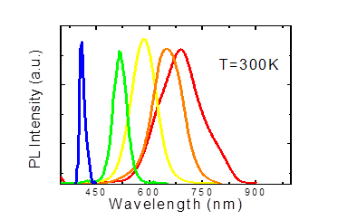
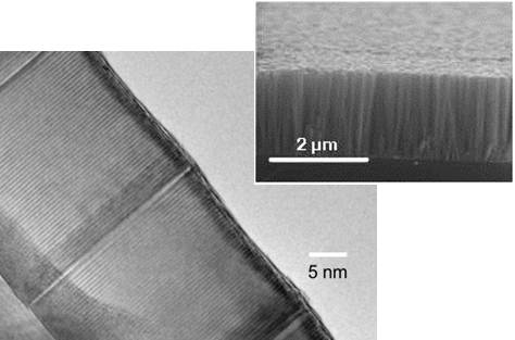
The overall objectives of this IRG are to investigate the epitaxial growth of GaN- and ZnO-based nanowires and quantum confined heterostructures and exploit these unique materials to study light-matter coupling processes and investigate the intrinsic properties of efficient wide-gap quantum emitters. We characterize defects, strain, polarization fields and optical properties of the nanostructures. Laser spectroscopy and quantum optical studies include the characterization of single photon properties, relaxation and decoherence rates, dynamics of hot carriers, and quantum and spin coherence phenomena. Strong coupling phenomena and polariton emission properties areinvestigated at high temperatures. It is important to add that while there is ongoing work on the growth of nanowires and quantum structures, their intrinsic properties are yet to be elucidated; similarly very little work has been reported on the use of wide-bandgap GaN and ZnO-based heterostructures for the studies listed above. The characteristics of light-emitting diodes and lasers made with quantum dot and nanowire gain regions are being investigated. For example, the role of Auger recombination, defects and carrier leakage in the performance of light-emitting diodes, which lead to efficiency roll-off, or “droop” is being examined theoretically and experimentally. This is a serious shortcoming in nitride-based LEDs, which impacts the progress of solid-state lighting.
Exploring Correlated and Topological Quantum Phases in Twisted Bilayer Crystals (Seed 11)
Principal Investigator
Sanfeng Wu, Assistant Professor of Physics
Seed start and end dates: November 1, 2018 - October 31, 2019
One of the remarkable contributions of graphene research over the past decade is to teach us how to realize high quality 2D electronic systems in the simplest settings – materials with only a single atomic layer. In such atomic monolayers, the quantum electronic properties can be unprecedently controlled through external fields or van der Waals interface engineering. For instance, stacking two monolayer crystals in a twisted fashion can result in long wavelength Moiré patterns (Fig. 1A-C), which can significantly alter the electronic bands at low energies. At certain “magic” twist angles, the band can even be tuned to be very flat. In the case of graphene, this “twistronics” approach creates a flat band at an angle near 1.1o, leading to the observation of superconductivity. In general, it has pointed to a new, fascinating route to achieve flat bands and strong electron correlations without introducing any disorder, through controlling the stacking parameters of a van der Waals heterostructure.
An electronic flat band not only holds the promise to achieve high-Tc superconductivity, but also could lead to the observation of fractionalized quantum states at zero magnetic field. The latter requires the development of a flat band with strong spin-orbit coupling and non-trivial topology. However, graphene itself has very weak spin-orbit coupling, and its electronic band is topologically trivial at finite temperatures. Hence, it is of great interest to apply the twistronics approach to other 2D crystals, especially those with non-trivial topology.
Harnessing Mixed Anion Systems to Create Novel Magnetic Properties
Precise synthetic control of the local electronic structure of metal centers within materials offers the potential to engender exotic physical properties. In particular, tuning the electronic structure of metal centers enables the creation of strongly correlated electron systems, enabling researchers to ask fundamental questions about magnetism and superconductivity. Within this Seed, a team of researchers is working on harnessing classes of mixed anion systems to discover and manipulate magnetic and superconducting properties of materials. Currently, numerous materials offer the potential to host topologically interesting phenomena, thereby tying into the NSF goal of creating new quantum materials. Indeed, any material that offers fundamental excitations that differ from previously studied particles is of interest within this area.
Northwestern University Materials Research Science and Engineering Center (2000)
The Materials Research Science and Engineering Center (MRSEC) at Northwestern University supports an interdisciplinary research program on materials with an emphasis on the nanoscale. The theme of the MRSEC is "Advancing Materials Research and Education to Improve the Quality of Life". Research is carried out in four interdisciplinary research groups, with appropriate seed projects. Within IRG 1 the Center focuses on nanostructured materials for chemical and biological sensing with the aim to develop and characterize new materials for use in making chemical and biological sensors for environmental applications. Within IRG 2 complex oxides are investigated to use materials design and synthesis in order to develop new thin film ceramic materials required for advanced photonic applications. The work in IRG 3 uses and interdisciplinary approach to develop a scientific basis for the synthesis and processing of new types of environmentally benign polymers. Finally, IRG 4, which is concerned with the architecture, transport, and binding in molecular crystals, polyelectrolyte nanocomposites, and nanoscale structures, is focused on new materials and the design of new molecular assemblies with ultimate potential applications to batteries, fuel cells, and molecular electronics. The Center features a strong pre-college educational program, including the widely disseminated Materials World Modules (MWM), as well as outstanding undergraduate and graduate educational opportunities. Of particular interest is the Master's Materials Technology Program which prepares graduates to teach materals science concepts at the community college level.
Functional Organic-Inorganic Electronic Interfaces
 Interfaces between organic and inorganic materials are now critical to many areas of science and technology, impacting such diverse areas as efficient solid-state lighting, consumer electronics and chemical/biological sensing. Yet there remains very little understanding of how to predict and control the chemical and physical properties of these interfaces at the nanoscale. The goal of our IRG on Functional Organic-Inorganic Electronic Interfaces is to develop the ability to design, fabricate and characterize interfaces between inorganic materials and organic molecular structures in such a way as to have complete control over their structural and electronic properties.
Showing 1071 to 1080 of 2596