Highlights
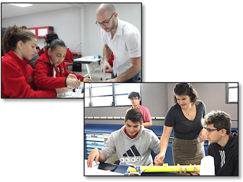
Teaching and Inspiring Students in Puerto Rico
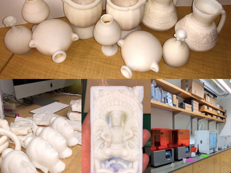
Oriental Institute Mobile Museum Project
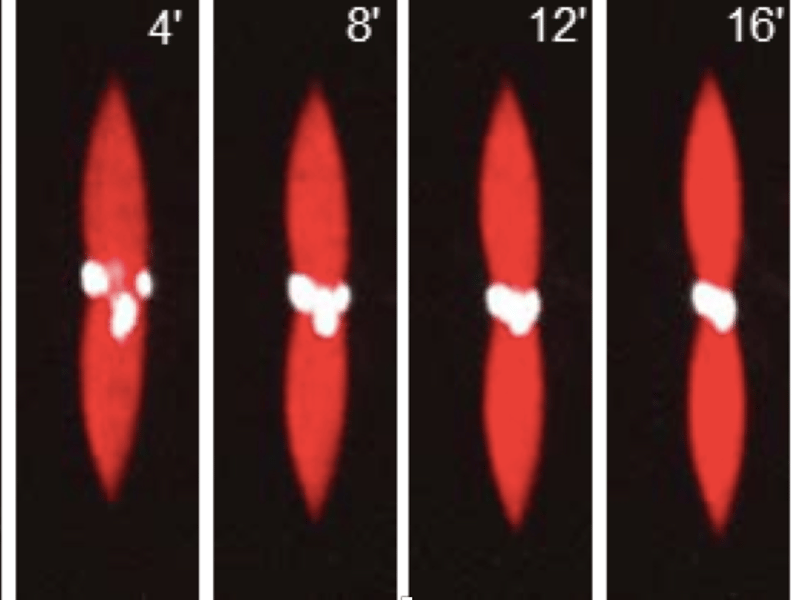
Self-organizing motors divide active liquid droplets
Kimberly L. Weirich (James Franck Institute, University of Chicago) Kinjal Dasbiswas (James Franck Institute, University of Chicago) Thomas A. Witten (James Franck Institute & Dept. of Physics, University of Chicago) Suriyanarayanan Vaikuntanathan (James Franck Institute & Dept. of Chemistry, University of Chicago) Margaret L. Gardel (James Franck Institute & Dept. of Physics, University of Chicago)
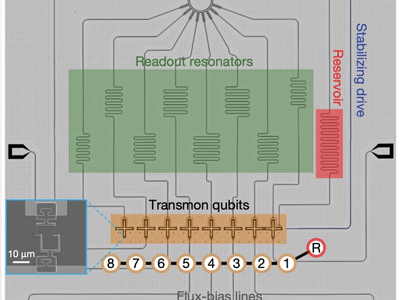
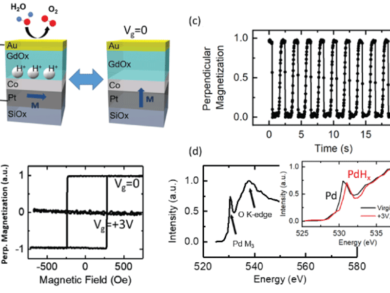
Building strongly interacting photonic materials
Ruichao Ma (University of Chicago) Brendan Saxberg (University of Chicago) Clai Owens (University of Chicago) Nelson Leung (University of Chicago) Yao Lu (University of Chicago) Jonathan Simon (University of Chicago) David I. Schuster (University of Chicago)
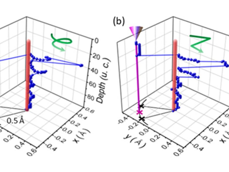
Subatomic Channeling and Spiraling Electron Beams in Crystals
K. Andre Mkhoyan, University of Minnesota
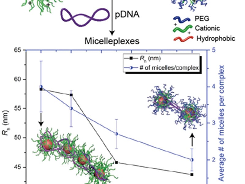
ABC Micelleplexes: Precise Compaction and High Colloidal Stability
Timothy Lodge and Theresa Reineke, University of Minnesota
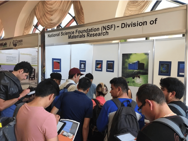
NSF-MRSEC Booth at the International Materials Research Congress
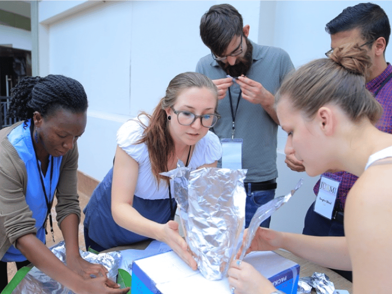
Joint Undertaking for an African Materials Institute (JUAMI)
Showing 381 to 390 of 1451