Highlights
Jul 10, 2017
Harvard University
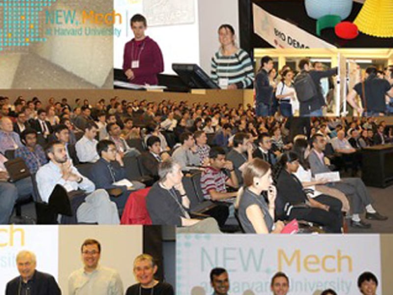
NEW.Mech Workshop for the New England Mechanics Community
Katia Bertoldi (MechEng), James R. Rice (EnvSciEng and Geol) and Christopher H. Rycroft (ApplMath)
The MRSEC co-sponsored NEW.Mech, a one-day workshop held in October 2016 at Harvard. The annual conference brings together researchers to explore new directions in the mechanics of materials and structures.
Jul 3, 2017
Yale University
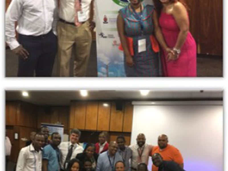
Developing a Solar Outreach Program for Haiti
Andre Taylor, Yale University
A Solar Outreach Program for Haiti is comprised of an interdisciplinary team of students, professors, university partners, and non-governmental organizations whose goal is to design and build Integrated Energy Centers in energy scarce regions. This year, the program developed a business plan, located investors, and submitted several grant proposals.
Jul 3, 2017
Yale University
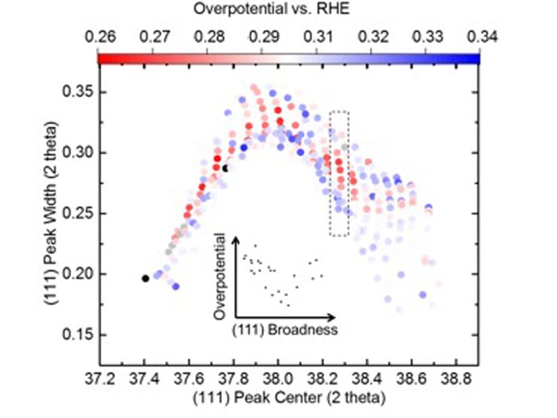
Combinatorial screening of metallic glass electrocatalysts for the oxygen reduction reaction
Andre Taylor and Jan Schroers, Yale University
Due to enormous challenges associated with theoretical modeling of multicomponent alloys, there are no reliable theoretical predictions available for their composition-dependent properties and structures. Taylor and Schroers have proposed to use combinatorial materials science to address this challenge.
Jul 3, 2017
Yale University
New Haven Science Fair Participation
Schwarz, Yale University
CRISP continued its interactions with industrial companies that aim to commercialize broadly new and simpler approach for force microscopy measurements. Separately, CRISP continued to train graduate students in research, writing, and presentation skills by providing the opportunity to attend a number of international conferences.
Jul 3, 2017
Yale University
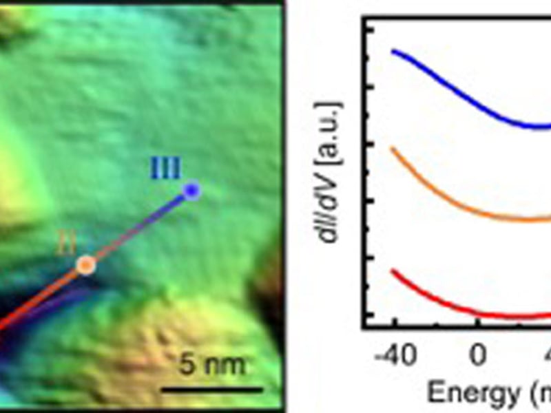
Tailoring Topological Surface States
Schwarz, Altman, Walker, Ismail-Beigi, and Ahn, Yale University
Topological crystalline insulators feature conducting surface states for electrons whose existence is protected by crystal symmetry. Scanning probe microscopy experiments on SnTe reveal that such metallic topological states can coexist next to semiconducting regions.
Jun 29, 2017
Columbia University in the City of New York
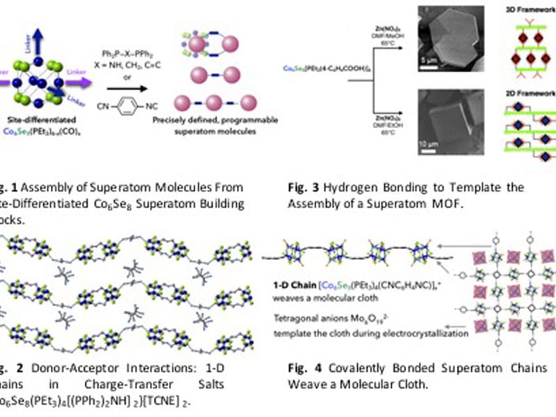
Programming Dimensionality in Superatomic Materials
Colin Nuckolls, Columbia University Center for Precision Assembly of Superstratic and Superatomic Solids
Featured as one of the “Ten Ideas That Will Change the World” in Scientific American in 2016, the discovery of assembling site-differentiated, atomically precise clusters into dimensionally controlled materials opens a new way to design and program a next generation of functional nanomaterials.
Jun 29, 2017
Columbia University in the City of New York
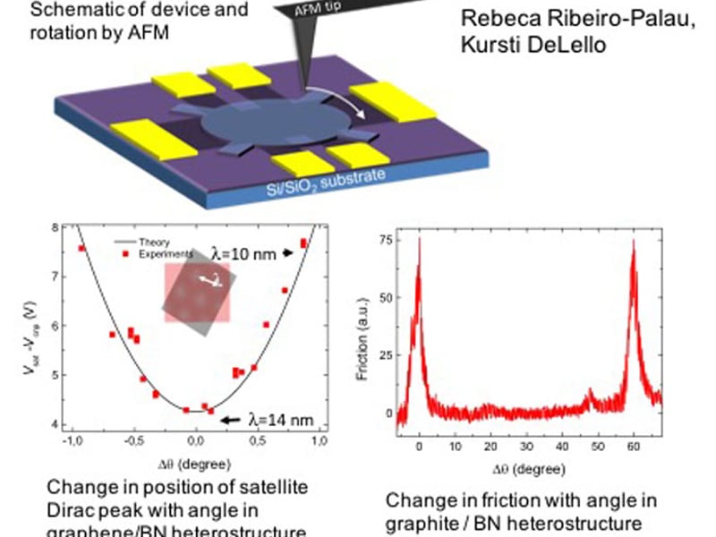
Rotating van der Waals Heterostructures
Cory Dean, Columbia University Center for Precision Assembly of Superstratic and Superatomic Solids
IRG1 of the Columbia MRSEC seeks to understand the behavior of van der Waals heterostructures created by assembly of atomically thin layered materials. One important question in this effort is how the relative orientation between the layers affects multiple properties.
Jun 27, 2017
Duke University
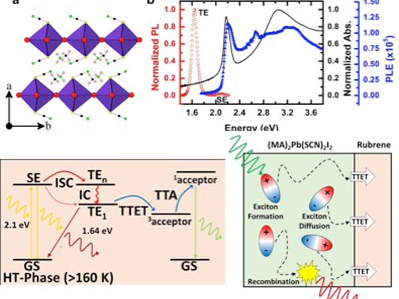
Efficient Generation of Long-lived Triplet Excitons in 2D Hybrid Perovskites
Stefan Zauscher, Director, Research Triangle MRSEC
Most recent work on hybrid organic-inorganic perovskites is focused on solar cell applications. Hybrid perovskites, however, provide a flexible platform for materials design, with prospects for many different applications.
Jun 27, 2017
Duke University
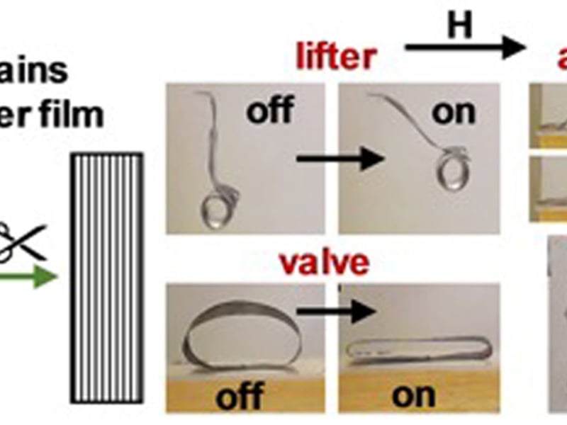
Magnetic Particle Chains for Directionally Controlled Actuation of Soft Robots
Stefan Zauscher, Director, Research Triangle MRSEC, Duke University
Researchers at North Carolina State University and Elon University have developed soft robots based on magnetic field-directed self-assembly of magnetic particles into chains embedded in elastomer films.
Jun 21, 2017
Brandeis University
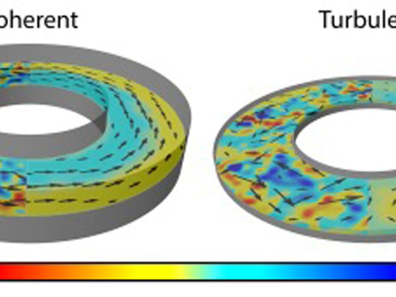
Coherent Flows in Confined 3D Active Isotropic Fluids
Seth Fraden and Zvonimir Dogic, Brandeis University
Navier-Stokes equations dictate that the conventional fluid flows only in response to an externally imposed gradient in stress or a body force. We developed a novel active fluid that is comprised of microtubules and energy consuming molecular motors kinesin.
Showing 511 to 520 of 1451