X-ray Facility
Faculty Director:
safinya [at] mrl [dot] ucsb [dot] edu (Professor Cyrus Safinya)
Technical Director
youli [at] mrl [dot] ucsb [dot] edu (Dr. Youli Li)
Staff Research Associate
miguelz [at] mrl [dot] ucsb [dot] edu (Miguel Zepeda)
Location
MRL 1012,1032 and CNSI (Elings Hall) 1409 (UCSB Campus Map)
The MRL X-ray Facility provides state-of-the-art x-ray diffraction tools for characterizing structural properties of a wide range of materials including metals and composites, polymers and biological materials, and electronic and optoelectronic materials in the lengthscale range of 0.1 nm - 100 nm. As a key research asset of the MRL, the x-ray facility is accessible by MRL researchers as well as off-campus academic groups and industrial users. In addition to maintaining an array of commercial and custom-built specialty instruments, the facility staff also conducts active research in developing new x-ray imaging methods and instrumentation to advance the capabilities of x-ray characterization techniques.
Management, operation and acquisition of equipment for the X-ray facility is supported by the Materials Research Laboratory: an NSF Materials Research Science and Engineering Center (MRSEC).
Floating Zone Furnace
Our floating zone furnace (Crystal Systems Inc.Model FZ-T-12000-X-S) employs four halogen optical lamps to achieve crystal growth temperatures up 2100ºC at pressures of 10-8 - 10 bar and is particularly suited to the growth of oxide single crystals. It permits growth of both congruent and incongruent melting systems. This system is utilized to prepare crystals with high spin polarization, as well as ferroelectric materials.
MRL UCSB Polymer Characterization Facility
Facility Director
hawker [at] mrl [dot] ucsb [dot] edu (Professor Craig Hawker)
Technical Director
Dr. Rachel Behrens, rachel [at] mrl [dot] ucsb [dot] edu
Training
Users of the MRL Synthesis and Characterization Laboratory are required to go through two levels of training before they are authorized to perform data collection independently. The training consists of
- General lab safety training, provided by the UCSB Environmental Health & Safety Department (EH&S).
- Instrument training, conducted by the manager Rachel (rachel [at] mrl [dot] ucsb [dot] edu) or an authorized user delegated by the laboratory manager.
Scheduling for Instruments
X-ray Diffraction Facility
A custom-built wide angle x-ray scattering (WAXS) system with a Huber 4-circle goniometer capable of accommodating large sample chambers (such as temperature-controlled ovens), this diffractometer is used routinely for structural characterization of liquid crystalline, polymeric and biological materials, x-ray reflectivity measurements on thin films, and high-resolution powder diffraction of polycrystalline materials.
High Resolution Electron Microscopy and Surface Structure Facility
This facility provides unique equipment to investigate the atomic scale structure of both the surface and sub-surface region of a sample combined with in situ growth and chemical characterization.
Surface Analysis and nano-Scale Imaging in the Micron Technology Foundation, Inc. Microscopy Suite
This USTAR-funded facility includes optical, electron, X-ray and ion microscopes, along with specialized analysis techniques to study surface topography, surface chemistry and even optical and dielectric properties of materials. The suite co-locates the MRSEC shared user facilities, the instruments of the Surface Analysis Lab, and also the Health Sciences Center (HSC) Electron Microscopy Core (EM for clinical pathology). Professional staff support includes PhDs in engineering, physics (laser optics, electron optics), physical & analytical chemistry, and cellular biology.
The ~5,300 square foot microscopy suite is the nexus point in the multidisciplinary facility, being strategically and metaphorically placed as a bridge between the engineering / science campus, and the medical school. Within the building, it is located between the research tower and the cleanroom. The microscopy suite is where these diverse researchers from all over campus physically bump into each other in a suite of tools designed to serve both hard and soft materials. This is where problem-solving engineers and life science researchers working on micro-and nano-scale devices meet life scientists who have ideas for quality-of-life-improving applications; but who need engineered solutions. We engineer having these people run into each other, and look for the magic that results!
LRSM Computing Facility
Location: South Bank Data Center
Supervisor/Coordinator: Robert A. Riggleman, Chemical and Biomolecular Engineering; Andrea J. Liu, Physics and Astronomy
Contact: Daniel Widyono
Email: [email protected]
Rob Riggleman, [email protected]

The LRSM Computing Facility is part of the Walnut High Performance Computing cluster (walnut.pics.upenn.edu) and is a shared facility for theory, simulation, and data analysis for projects supported by the MRSEC. The cluster consists of 62 nodes, each with four Intel E5-4620 8-core processors (at 2.2 or 2.6GHz) and 64GB RAM. The nodes are connected by a low-latency Infiniband network to allow for efficient parallelization. The MRSEC owns approximately 30% of the Walnut Cluster, giving MRSEC users priority access to 568 compute cores, and limited access to the entire cluster during periods of reduced utilization.
Rheology Center
Location: LRSM Building
Supervisor/Coordinator: Paul A. Janmey, Karen I. Winey, Paulo Arratia and Arjun G. Yodh
Equipment:
Confocal Rheometer
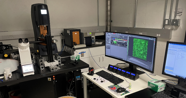
Faculty advisor: Paulo E. Arratia The LRSM possess a state-of-the-art confocal rheometer microscope equipped with a confocal microscope (Leica Stellaris) and a stress-controlled rheometer (TA Instrument DHR-3). This apparatus allows researchers to impose precise kinematic deformation onto a desired material while simultaneously characterizing the fluid microstructure and measuring the bulk fluid response.

The confocal microscope (Leica Stellaris) works by packaging a variable wavelength laser and a photo-multiplier detector into a single unit. With high precision, rapid motion of the objective (above 8KHz), achieved by harnessing a piezoelectric element, three dimensional (3D) scans (256 x 256 x 100 voxels) of a material’s structure can be created. Of key importance is that the scan be completed more rapidly than the time scales of imposed stress from the rheometer, ensuring minimal sample motion during the scan.
A TA Instrument DHR-3 rheometer is integrated to the confocal microscope. This hybrid rheometer is amenable to imaging via an off-the-shelf accessory and in-house optical manipulation. The DHR-3 provides good measurement quality for a variety of rheological tests and can resolve a torque range of 0.5nN.m to 200mN.m, with changeable geometries adding another two orders of magnitude to the range of detectable stresses. This is an important feature in providing enough dynamical rage from low to high viscosity samples.
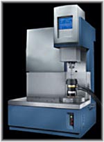
TA Instruments RFS II
 Faculty advisor: Paul A. Janmey This facility is capable of characterizing both the structure and flow properties of simple and complex fluids. It can solve the most demanding fluid rheology problems including dynamic oscillatory and shear rate controlled measurements on low viscosity structured fluids. It is equipped with:
- Peltier plate temperature control (from -30oC to 150 oC)
- Recirculating fluid bath (from -10 oC to 140 oC)
- Forced convection oven
- Torque ranges from 0.002 to 1000 g.cm
- Frequency ranges from 10-5 to 500 rad/sec
Bohlin Gemini
 Faculty advisor: Arjun G. Yodh, facility contact: Somayeh Farhadi
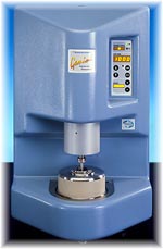
The Bohlin Gemini rheometer is optimized for both stress controlled and strain controlled measurements. Technical features include a broad torque range, which extends to 200 mNm. The high-resolution torque mapping system applied to Bohlin’s low bias air bearing technology allows low torques to be set extremely accurately. The Bohlin is ideal for stress or strain controlled measurements of viscoelastic fluids with shear modulus as low as 1mPa. Couple with Nikon Eclipse 200/Confocal VT Eye microscopy for in-situ imaging during shearing (see details below)
Haake CaBER
 Faculty advisor: Arjun G. Yodh, facility contact: Somayeh Farhadi
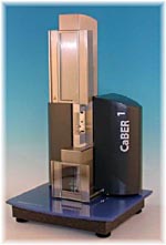
The Haake CaBer (capillary break-up extensional rheometer) provides valuable information about a material’s extensional properties that rotational rheometers cannot provide. With the CaBER, stringiness, filaments break-up time and extensional viscosity can be quantified.
Nikon Eclipse 200/Confocal VT Eye
Faculty advisor: Arjun G. Yodh, facility contact: Somayeh Farhadi
Inverted light microscope, capable of fluorescence microscopy. This microscope is attached to a VisiTech ‘VT-Eye’ confocal setup, and Bohlin Gemini rheometer. VisiTech ‘VT-Eye’
- 30 images per second (512 x 512 pixels); up to 400 images/s for reduced field of view
- Ultra-fast 3D acquisition: 256 x 256 x 100 pixel 3D image, 1 per second
- Z-scan up to 100 microns with 100 nm resolution
- Multi- wavelength excitation laser, at 488, 569 and 633 nm
- Reflection mode capability
- VoxCell software for easy control and data management
Instron Model 5564 Table Mounted Materials Testing System
 Faculty advisor: Karen I. Winey This facility is capable of performing tensile, compression, peel, and flexural tests on most materials and components. It is equipped with:
- 2 tension/compression load cells with capacity of 2kN and 10N, respectively.
- 1 rigid coupling.
- 1 micro 3-point bend fixture.
- 2 stainless steel tensile grips with 100lb capacity.
- 1 double-walled saline immersion vessel with digital temperature controller.
Showing 291 to 300 of 2599